2019年11月18日星期一

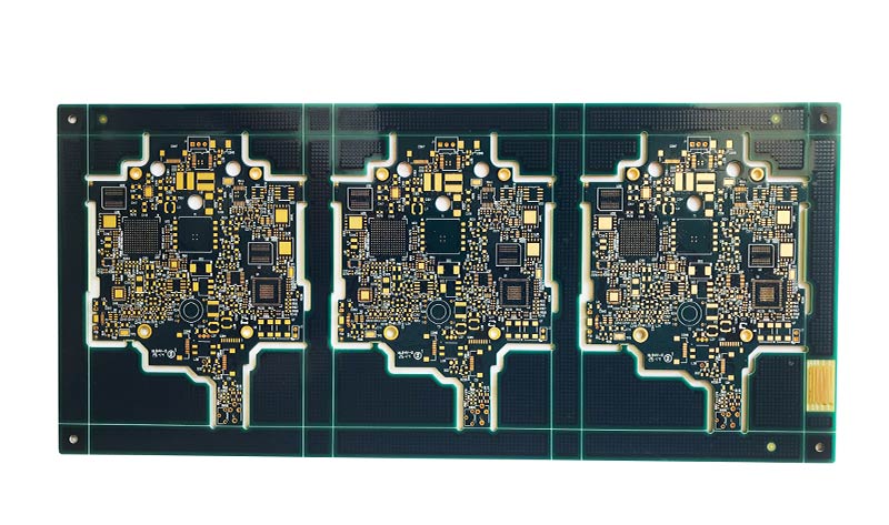
Printer motherboard pcba pcb assembly

Our products include HDI board, heavy copper board, backplane board,Blind & Buried PCB semiconductor test board, high frequency board and rigid-flex board, etc., to meet customers' various demand. Our products are widely used in communication, medical equipment, industrial control, power supply, consumer electronics and aerospace, automobile industry, etc.
TOPFAST is a professional and reliable one-stop PCB solutions provider for customers specialized in manufacturing quick turn prototypes and small volumes. With high quality and on-time delivery products we won the market's wide acclaim. We will continue to focus on customer satisfaction, along with "high quality “and "fast delivery", we will become a PCB service provider worthy of customer trust.
Order Conditions
Standard Delivery Date
The fastest Delivery Date
Prototype (<20 pcs)
 2 days
 8   hours
Small Volum (20-100 pcs)
 3 days
 12 hours
Medium Volum(100-1000 pcs)
 6 days
 24 hours
Mass productions (>1000 pcs)
 Depends on BOM
 Depends on BOM

2019年11月14日星期四

What Is A Printed Circuit Board?

What is a printed circuit board? Printed circuit boards are the providers of electrical connections to electronic components. It has been developed for more than 100 years; its design is mainly layout design; the main advantage of using the circuit board is that it greatly reduces wiring and assembly errors, and improves the automation level and production labor rate. So what is the printed circuit board? The PCB Board For Industrial Control Supplier will come to tell you.

Printed circuit boards can be divided into single-panel, double-panel, four-layer, six-layer, and other multi-layer boards according to the number of circuit boards. Common multi-layer boards are generally 4-layer boards or 6-layer boards, and complex multi-layer boards can reach more than a dozen layers. It has the following three main types of division:

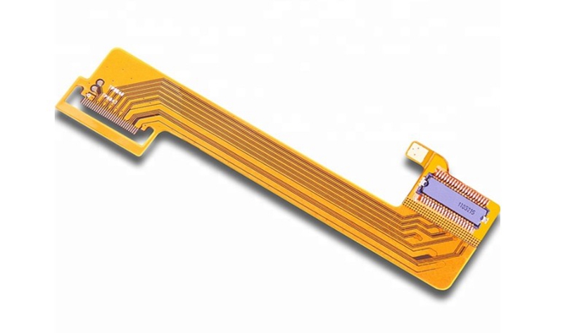
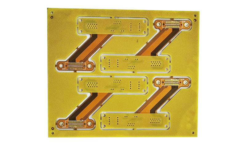
2 Sided Flexible Circuit Board Material

2 Sided Flexible Circuit Board Material

Single panel: On the most basic PCB, the parts are concentrated on one side and the wires are concentrated on the other side. Since the wire only appears on one side, this PCB is called a single-sided. Because single-panel has many strict restrictions on the design line (because there is only one side, the wiring can not cross and must be around the path), so only the early circuit used this type of board.

Double panel: This board has wiring on both sides, but to use the two sides of the wire, you must have the appropriate circuit connection between the two sides. The "bridge" between such circuits is called a via. The via hole is a small hole filled or coated with metal on the PCB, which can be connected to the wires on both sides. Because the area of the double panel is twice as large as that of the single panel, and because the wiring can be interlaced (can be wound around the other side), it is more suitable for circuits that are more complex than single panels. There are many Double Sided PCB Wholesaleon the market.

Multilayer board: In order to increase the area that can be routed, the multi-layer board uses more single or double-sided wiring boards. Using a double-sided inner layer, two single-sided outer layers or two double-sided inner layers, two single-sided outer printed circuit boards, alternating between the positioning system and the insulating bonding material and conductive patterns Printed circuit boards that are interconnected according to design requirements become four-layer, six-layer printed circuit boards, also known as multilayer printed wiring boards. The number of layers in the board represents several separate layers of wiring, usually with an even number of layers and containing the outermost two layers. Most of the motherboards are 4 to 8 layers of structure, but technically they can achieve nearly 100 layers of PCB. Large supercomputers mostly use quite a few multi-layer motherboards, but because such computers can already be replaced by clusters of many common computers, super-multilayer boards have gradually disappeared.

Because the layers in the PCB are tightly coupled, it is generally not easy to see the actual number, but if you look closely at the motherboard, you can still see it. Classified according to soft and hard: divided into ordinary circuit boards and flexible circuit boards, such as common 2 Sided Flexible Circuit Board Material. The raw material of the PCB is a copper clad laminate which is a substrate material for making a printed circuit board. It is used to support various components and to achieve electrical or electrical insulation between them. A PCB is simply a thin plate with integrated circuits and other electronic components. It will appear in almost every electronic device. Since the printed circuit board is not a general terminal product, the definition of the name is slightly confusing. For example, the motherboard for the personal computer is called the motherboard, and cannot be directly called the circuit board. Although there is a circuit board in the motherboard, It's not the same, so when you evaluate the industry, you can't say the same thing. For example, because the integrated circuit parts are mounted on the circuit board, the news media called him an IC board, but in essence he is not equivalent to a printed circuit board. We usually say that the printed circuit board refers to the bare board - that is, the board without the upper components.

2019年11月8日星期五

Five Principles Of Pcb Board Technology

With the rapid development of mobile phones, electronics, and communications industries, the PCB circuit board industry continues to grow and grow rapidly. For the number of layers, weight, precision, materials, line width, line spacing, and reliability of circuit boards. The requirements are getting higher and higher.

So what principles should be followed for PCB board processing? Multilayer Flexible PCB Factory will to tell everyone.
1. Printed wire width selection: The minimum width of the printed wire is related to the current flowing through the wire: The line width is too small, the resistance of the printed wire is large, and the voltage drop on the wire is large, which affects the performance of the circuit. Wide, the wiring density is not high, the board area increases, in addition to increasing the cost, it is also not conducive to miniaturization. If the current load is calculated at 20A/mm 2 , when the thickness of the copper foil is 0.5MM, (generally so much,) Then 1MM (about 40MIL) line width current load is 1A, therefore, the line width is 1-2.54MM (40--100MIL) can meet the general application requirements, the ground wire and power supply on the high-power equipment board, according to the power The size can be appropriately increased, and in the low-power digital circuit, in order to increase the wiring density, the minimum line width can be satisfied by taking 0.254 - 1.27 MM (10 - 15 mil). In the same circuit board, the power line and the ground line are thicker than the signal line.

2. Line spacing: When it is 1.5MM (about 60MIL), the insulation resistance between lines is greater than 20M ohms, and the maximum withstand voltage between lines can reach 300V. When the line spacing is 1MM (40MIL), the maximum withstand voltage between lines is 200V. Therefore, on a circuit board with medium and low voltage (line voltage not greater than 200V), the line spacing is 1.0--1.5MM (40--60MIL). In low-voltage circuits, such as digital circuit systems, it is not necessary to consider the breakdown voltage. The production process allows, can be small.

3. Pad: For a 1/8W resistor, a pad lead diameter of 28 MIL is sufficient, while for a 1/2 W, the diameter is 32 MIL, the lead hole is too large, and the pad copper ring width is relatively reduced. , causing the adhesion of the pad to decrease. It is easy to fall off, the lead hole is too small, and component mounting is difficult.

4. Draw circuit border:
The shortest distance between the border line and the component pin pad can't be less than 2MM (usually 5MM is reasonable), otherwise it is difficult to cut.
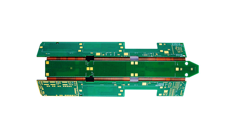
Rigid Flex PCB Board Manufacture

Rigid Flex PCB Board Manufacture

5. Component layout principles:
(1) General principle: In the Rigid Flex PCB Design, if the circuit system has both digital and analog circuits and large current circuits, it must be laid out separately, so that the matching between the systems is minimized in the same type of circuit, according to the signal Flow direction and function, block, partition and place components.
(2) Input signal processing unit, the output signal drive component should be close to the edge of the board, so that the input and output signal lines are as short as possible to reduce the interference between the input and output.
(3) Component placement direction: Components can only be arranged in both horizontal and vertical directions. Otherwise, the components should not be used.
(4) Component spacing. For medium-density boards, small components, such as small power resistors, capacitors, diodes, etc., the spacing between discrete components is related to the plug-in, soldering process. When soldering, the component spacing can be 50-100 MIL (1.27-- 2.54MM) can be larger by hand, such as 100MIL, integrated circuit chip, the component spacing is generally 100--150MIL.
(5) When the potential difference between components is large, the component spacing should be large enough to prevent discharge.
(6) The hour hand circuit component is as close as possible to the clock signal pin of the microcontroller chip to reduce the length of the connection of the clock circuit. It is better not to route the wire below.

The above is about PCB circuit board design process, if you are interested in PCB circuit board, you can contact us, we have Rigid Flex PCB Board Manufactureand PCB design, we can certainly meet your needs, welcome your purchase.

2019年11月5日星期二

What Are The Characteristics Of Good Quality PCB Boards?

The PCB circuit board is an important electronic component, a support for electronic components, and a carrier for electrical connection of electronic components. After the electronic equipment adopts the printed board, due to the consistency of the same printed board, the manual wiring is avoided, and the electronic components can be automatically inserted or mounted, automatically soldered, and automatically detected to ensure the quality of the electronic equipment. Increase labor productivity, reduce costs, and facilitate maintenance. The judgment of the quality of the PCB board is generally based on the appearance of the judgment, but depending on the experience, the quality of the PCB board is very important, so what are the characteristics of the good quality PCB board? As a PCB Board For Industrial Control Supplier, we will arrange some professional advice for you.

1, 25 micron hole wall copper thickness
Benefits: Enhanced reliability, including improved z-axis resistance to expansion. If this is not the case, there will be blowholes or degassing, electrical connectivity problems during assembly (inner layer separation, hole wall fracture), or failure under load conditions in actual use. IPCClass2 (the standard used in most plants) requires 20% less copper plating.

2, no welding repair or open circuit repair
The perfect circuit ensures reliability and safety, no maintenance and no risk. If it is not repaired properly, it will cause the board to open. Under load conditions (vibration, etc.) there is also a risk of failure, which may cause malfunction in actual use.

3. Strictly control the service life of each surface treatment
Has solderability, reliability, and reduces the risk of moisture intrusion. Regardless of this factor, soldering problems may occur due to metallographic changes in the surface treatment of old boards, and moisture intrusion may result in delamination, inner layers and holes during assembly and/or actual use. Wall separation (open circuit) and other issues.

4. Cladding tolerance meets IPC4101 Class B/L requirements
Strict control of the thickness of the dielectric layer can reduce the expected deviation of electrical performance. When the requirements are not met, the electrical performance may not meet the specified requirements, and the output/performance of the same batch of components may vary greatly.

5. Define the solder mask material to ensure compliance with IPC-SM-840 ClassT requirements
“Excellent” inks for ink safety and ensuring solder mask inks meet UL standards. Inferior inks can cause adhesion, flux resistance and hardness problems. All of these problems can cause the solder mask to detach from the board and eventually lead to corrosion of the copper circuit. Poor insulation properties can cause short circuits due to unexpected electrical connectivity/arc. For example, Embedded Active Components PCB should meet this requirement in order to achieve its role.

6. Define tolerances for shapes, holes and other mechanical features
Strict control of tolerances can increase the dimensional quality of the product – improved fit, form and function. Failure to do so can cause problems during the assembly process, such as alignment/mating (the problem of press-fitting the needle is only found when the assembly is complete). In addition, there is a problem in mounting the base due to an increase in dimensional deviation.

7, the thickness of the solder mask, although the IPC has no relevant regulations
This improves electrical insulation properties, reduces the risk of flaking or loss of adhesion, and enhances the ability to withstand mechanical impact.

Rigid Flex PCB Design

Rigid Flex PCB Design

The above is a part of the introduction of the characteristics of good quality PCB boards that we introduce to you. Of course, there are many features of good PCB boards. If you have PCB requirements, you can contact us. We include PCB board and Rigid Flex PCB Design. Welcome everyone to come and buy.

2019年11月1日星期五

Introduction To OSP Process Of PCB Circuit Board

Find here details of Buried PCB Board on our website. Today we would like to talk about introduction to osp process of PCB circuit board.

Printed circuit board method for saving manufacturing cost.

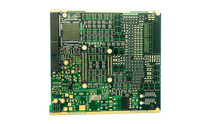
Buried PCB Board

Buried PCB Board


In order to make the cost of the PCB as low as possible, there are many factors shared by Industrial Control PCB Board Saler that must be considered:

The size of the board is naturally a focus. The smaller the board, the lower the cost. Part of the PCB size has become the standard, as long as the cost is reduced according to the size.

Using SMT will save you money than THT, because the parts on the PCB will be denser (and smaller).

On the other hand, if the parts on the board are dense, the wiring must be thinner and the equipment used should be relatively higher. At the same time, the materials used should be more advanced, and the wiring design must also be more careful, so as to avoid the problem that power consumption and the like may affect the circuit. The cost of these problems can be saved more than the reduction in PCB size.

The higher the number of layers, the higher the cost, but PCB with a small number of layers usually cause an increase in size.

Drilling takes time, so the fewer the guide holes, the better.

Buried holes are more expensive than via that run through all layers. Because the buried hole must be drilled before the joint.

The size of the holes in the board is determined by the diameter of the part pins. If there are different types of pin parts on the board, then because the machine can't use the same bit to drill all the holes, the relative time is spent, which also represents a relatively high manufacturing cost.

Electronic testing using flying probe detection is usually more expensive than optical. Generally optical testing is enough to ensure that there are no errors on the PCB.

All in all, the time and effort of manufacturers on the equipment is becoming more and more complicated. It is useful to understand the PCB manufacturing process, because when we compare motherboards, the board cost of the same performance may be different and the stability is different, which allows us to compare the capabilities of various vendors.

A good engineer can look at the motherboard design and know the quality of the design. You may not think so strong, but next time you get the motherboard or graphics card, you may wish to appreciate the beauty of PCB design!

If you want to know the PCB Price, feel free to contact us.

2019年10月29日星期二

The Difference Between PCB And PCBA

Find here details of Buried PCB Board on our website. Today we would like to talk about the difference between PCB and PCBA.
Our products include HDI board, heavy copper board, backplane board,Blind & Buried PCB semiconductor test board, high frequency board and rigid-flex board, etc., to meet customers' various demand. Our products are widely used in communication, medical equipment, industrial control, power supply, consumer electronics and aerospace, automobile industry, etc.
PCB is also what we call the circuit board circuit board. The PCB drawing is processed into a circuit board circuit board called PCB. The SMT (SMD) is applied to the empty board of the PCB, and the components required for the board are called PCBA. The board that has been affixed with components only needs to be assembled with the outer casing, debugged the program, and a complete electronic product is completed.

Rigid PCB Supplier
Rigid PCB

According to the survey, many small and medium-sized electronic product manufacturers have to avoid the trouble of contacting the patch manufacturers after purchasing PCB. More and more electronic product manufacturers will choose to let PCB manufacturers process patches at the same time as PCB production, or let patch manufacturers replace PCB. These two models, electronic product manufacturers, get the circuit board, you can directly assemble and use to produce the finished product. Many manufacturers that can only produce PCB, unconditionally processing PCBA, will lose customers who need simultaneous processing. Such customers choose manufacturers that have the ability to add at the same time, or choose a patch factory to let the patch factory purchase PCB. Many people may ask why the patch factory can purchase PCB, and why the PCB factory does not contact the patch factory. It is very simple for patch manufacturers to purchase PCB. They only need to provide customers with production drawings and production processes. Moreover, the PCB market price is very transparent and easy to purchase. PCB manufacturers do not understand the various components and prices. It is difficult to contact the patch factory for patch production, and only focus on the production PCB.

Since 2009, Rigid PCB Supplier has gradually expanded their plants while producing PCB and added PCBA processing lines. This one-step approach has been recognized by many electronics manufacturers. This method of simultaneous processing has advantages and disadvantages. Generation processors are increasing in profit margins, but at the same time the risks are increasing. The main reason is that the components required for each electronic product are different for the purchase of components for the customer. Even if the same product, the design drawings are different, and the components used are different. If the model purchased by the component is faulty, the board and components will be scrapped at the same time. The direct economic losses are also difficult to estimate. The increase in human and material resources is also inevitable. Under the pressure of market competition, the simultaneous processing of PCB and PCBA is also inevitable.

If you want to know about Multilayer PCB Price, welcome to contact us.

2019年9月27日星期五

Introduction To The Basic Structure Of The Flexible PCB

Here is a Multilayer Flexible PCB Factory talking about introduction to the basic structure of the flexible PCB.

If you want to know about Multilayer PCB Price, feel free to contact us.

When we are using Flexible PCB, do you understand its basic structure and know what it is made of? Let's take a split to let everyone have a simple understanding of the basic structure of the flexible circuit board.

Flexible PCB

Flexible PCB


Copper foil substrate (Copper Film)

Copper foil: Basically divided into electrolytic copper and rolled copper. Commonly used in thickness are 1oz 1/2oz and 1/3 oz.

Substrate film: common thickness is 1mil and 1/2mil.

Glue (adhesive): thickness depends on customer requirements.

Cover Film

Cover film protection film: for surface insulation. Common thickness is 1mil and 1/2mil.

Glue (adhesive): thickness depends on customer requirements.

Release paper: avoid the adhesive sticking to foreign objects before pressing; easy to work.

Reinforcement plate (PI Stiffener Film)

Reinforcement plate: Reinforces the mechanical strength of the FPC for easy surface mounting. Common thicknesses range from 3 mils to 9 mils.

Glue (adhesive): thickness depends on customer requirements.

Release paper: Avoid adhesive adhering to foreign objects before pressing.

EMI: Electromagnetic shielding film protects the circuit inside the circuit board from external interference (strong electromagnetic area or susceptible area).

Recognizing the basic structure of flexible circuit boards, we have an understanding of the flexible circuit boards. The above is a brief introduction. We welcome a brief understanding of the needs.