2019年8月29日星期四

How To Deal With Warped PCB Boards?

Here is Rigid PCB Manufacturer talking about hoe to deal with warped PCB board. If you have any idea about it, you can contact us and share your idea with us. Also, we have Rigid PCB Sale. If you need any information, you also can contact us.

Rigid PCB Sale
Rigid PCB Sale

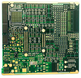
In the automated instrumentation line, if the printed board is not flat, it will cause misalignment, the components can not be inserted into the hole of the board and the surface mount pad, and even the automatic inserter will be damaged. The board on which the components are mounted is bent after soldering, and the component legs are difficult to trim. The board can't be installed in the chassis or the socket inside the machine, so it is very troublesome for the assembly factory to encounter the board. At present, printed boards have entered the era of surface mounting and chip mounting. The assembly plant's requirements for board warping must be more and more strict. Today, we will introduce how to handle warped PCB printed boards.

The well-managed factory, the printed board will be 100% flatness inspection during the final inspection. All unqualified boards will be picked out, placed in an oven, baked at 150 degrees Celsius and under heavy pressure for 3 to 6 hours, and naturally cooled under heavy pressure. Then, the plate is taken out by pressure relief, and the flatness is checked. This saves some of the boards, and some of the boards need to be pressed two to three times to level. If the above-mentioned anti-warping process measures are not implemented, some of the board drying pressure is useless and can only be scrapped.

2019年8月26日星期一

What are the Characteristics and Functions of Rigid PCB?

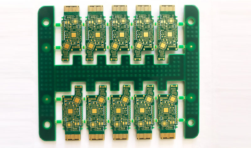
Here is Rigid PCB Supplier talking about the characteristics and functions of rigid pcb. Also, our company's Rigid PCB Sale has extended many countries in the world. If you have any question, you can contact us. Now let us learn about its features and functions.

Rigid PCB Sale
Rigid PCB Sale

Characteristics of Rigid PCB:
①It has high density. For more than 100 years, the high density of printed boards has grown with the integration of integrated circuits and advances in mounting technology.
②Designability. For the various performances of PCB (electrical, physical, chemical, mechanical, etc.), the design of printed boards can be realized through design standardization and standardization, with short time and high efficiency.
③Productivity. With modern management, it can carry out standardization, scale (quantity), automation and other production to ensure product quality consistency.
④High reliability. Through a series of inspections, tests and aging tests, the PCB can be reliably operated for a long period of time (usually 20 years).
⑤Testability. Established relatively complete test methods, test standards, various test equipment and instruments to detect and identify PCB product qualification and service life.

Rigid PCB function:
After the electronic equipment adopts the printed board, due to the consistency of the same printed board, the manual wiring is avoided, and the electronic components can be automatically inserted or mounted, automatically soldered, and automatically detected to ensure the quality of the electronic equipment. Increase labor productivity, reduce costs, and facilitate maintenance.

2019年8月22日星期四

Ethiopian Customer Visit

On June 26, 2019, the customer from Ethiopia, Bineyam Kahssay came to our factory to visit the factory. The account manager Albert led the customer to visit, mainly introducing the company's scale, development history, and the company's core competitiveness.
 After the visit, the company was quite satisfied and confirmed the cooperation relationship, and will send samples to the division later.
Ethiopian Customer VisitEthiopian Customer Visit

2019年8月19日星期一

What is the Production Process and Technical Standard of PCB Board?

Today Flexible Board Supplier like to tell you about the process and technical standard of PCB board.


Flexible Board Supplier

The production process of PCB Board:
Cutting, inner layer, lamination, drilling, copper sinking, wiring, drawing electricity, etching, solder masking, characters, spray tin, edge cutting, v cutting, fly test , vacuum packaging, etc.
The technical standard for welding:
Electrostatic protection during PCB board soldering: Leakage and grounding.
①Welding process: clean the components to be removed, heat the soldering iron with a soldering iron, clean the soldering feet with a soldering tin, remove the old components, correctly put new components, heat the soldering feet, move the solder wire, and remove the solder wire and remove the soldering iron.
②Check solder joints: whether the solder joints are round, shiny, firm, and whether it has solder joints with surrounding components.

2019年8月15日星期四

The Proofing Difficulties of Multilayer PCB Board

Due to the large number of layers in the multilayer PCB board, the user has higher and higher requirements for calibration of the PCB layer. Typically, the alignment tolerance between layers is controlled at 75 microns. So do you know the difficulties of China Multilayer PCB Board? Let us study together.
The Proofing Difficulties of Multilayer PCB Board


1. Difficulties in the production of internal circuit.
The multilayer pcb board adopts special materials such as high TG, high speed, high frequency, thick copper and thin dielectric layer, which puts high requirements on internal circuit fabrication and graphic size control. For example, the integrity of impedance signal transmission increases the difficulty of internal circuit fabrication.
The width and line spacing are small, the open circuit and short circuit increase, the short circuit increases, the pass rate is low; the thin line signal layer is more, the inner layer AOI leakage detection probability increases; the inner core board is thin, easy to wrinkle, poor exposure, easy to curl when etching machine; The high-level plate is mostly a system board, the unit size is large, and the product scrapping cost is high.
2. Difficulties in compression manufacturing.
Many inner and pre-cured sheets are superimposed, which are prone to defects such as sliding, delamination, resin voids and bubble residue in stamping production. In the design of the laminated structure, the heat resistance, pressure resistance, rubber content and dielectric thickness of the material should be fully considered, and a reasonable multi-layer circuit board material pressing scheme should be formulated.
3. Difficulties in drilling.
The use of high TG, high speed, high frequency, thick copper special plates increases the difficulty of drilling roughness, drilling burrs and drilling. The number of layers is large, the total copper thickness and plate thickness are accumulated, the drill is easy to break the knife; the dense BGA is more, the CAF failure problem caused by the narrow hole wall spacing; the plate thickness is easy to cause the oblique drilling problem.

If you also have any other difficulties, please contact us 18 Layers Rigid PCB Board Exporter, who can give you a professional guide.

2019年8月12日星期一

Understand The Consumable Parts On The Board During Maintenance

Here is Rigid Pcb Manufacturer talking about The Consumable Parts On The Board During Maintenance.
If you have any idea about Pcb Buried Components, welcome to contact us and discuss.
1. The most unreasonable design is the most troublesome
Any circuit board can't be perfected in design, and it has its own inherent defects and deficiencies. This is innate. When the equipment leaves the factory, it implies a certain fault that must occur when it is used. The weakness of these structures is sometimes the immaturity of the design. Sometimes the quality of the selected materials is not enough. Does the manufacturer know the weaknesses of this structure? Some know it, but it is unavoidable. 
Why do you say this? First of all, this is a question of whether the so-called fish and bear's paw can have both. In general, the better the quality of the device, the larger the component, the better, because the larger the component, the thicker the pin, the stronger it is. In reality, people are demanding smaller and more devices, more and more functions, and more power. The larger, the more contradictory; secondly, the longer the design time, the more the product will be perfect, but in fact, the manufacturer can't do it, and the product update speed is getting faster and faster. The faster the update, the more time the vendor has to test the performance of the product, the sacrifice is the quality of the product. Moreover, from another perspective, the production of equipment that is not bad for decades means the bankruptcy of the manufacturers. For our maintenance industry, repairing the boards that are not bad for decades means unemployment. So, what is the unreasonable design of industrial boards? The first is the heat dissipation problem. Many circuit board damages are caused by poor heat dissipation design, followed by the copper foil wire of the printed board. The copper foil of the poor quality circuit board power supply line is very thin, and it is easy to blow due to overcurrent. So that the motherboard can not work.
Rigid Pcb Manufacturer
2. The use of frequent places is prone to failure
 When repairing VCDs and DVDs, home appliance masters know that as long as the machine does not read the disk, it is a bad laser head, because the bald head needs to be illuminated, focused, tracked, and left and right to feed. As long as the machine works, it will Busy, this kind of "willing to sacrifice" spirit will one day "sick down", the same circuit board, for example, industrial circuit board drive motor, shaft, switch power supply switch, common buttons on the operation panel, etc.

2019年8月8日星期四

The Difference between Rigid PCB Design and Flex PCB Design

Do you know Rigid Flex PCB Design considerations? What's the differences between between Rigid PCB Design and Flex PCB Design? Today let us Rigid Flex PCB Manufacturer tell you.
Most of the design elements of rigid PCB have been applied to the design of flexible PCB. However, there are other new elements that need attention.

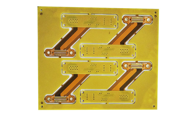
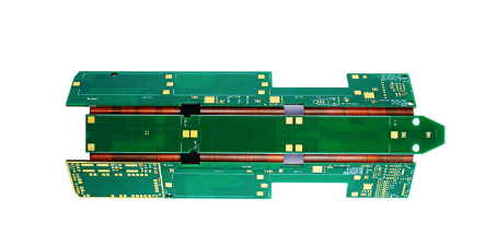
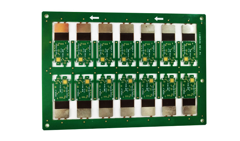
Metal Stiffener Rigid-Flex PCB

 Metal Stiffener Rigid-Flex PCB
1. Current carrying capacity of the wire
Because flex PCB have poor heat dissipation (compared to rigid PCB), sufficient wire width must be provided. When some wires carrying large currents are placed face to face or adjacent to each other, additional wire width or spacing must be given in consideration of the problem of heat concentration.

2. Shape
Wherever possible, rectangles should be preferred wherever possible, as this would result in better substrate savings. There should be enough free margins near the edges, depending on the possible remaining space of the substrate.

In shape, the inner corner should appear to be circular; the pointed inner corner may cause tearing of the panel.

Smaller wire widths and spacing should be minimized as much as possible. If the geometric space allows, the thin wires that are closely packed should become wide wires. The wires that terminate at the plated through holes or component mounting holes should be smoothly searched into the pads. As a general standard, any change from straight line to image angle or different line width must be as smooth as possible. Sharp corners will naturally concentrate stress and cause wire failure.

3. Flexibility
As a general standard, the bend radius should be designed to be as large as possible. The use of thinner laminates (for example: 50μm copper foil instead of 125μm copper foil) and wider conductors can better increase the likelihood of more cyclic bending. Single-sided flexible PCB typically show better performance for a large number of bending cycles.

4. Pad
Around the pad, there is a change from a flexible material to a rigid material. This area is more likely to break the conductor. Therefore, the pads should be avoided in areas where bending is likely to occur. The general shape of the pad should be like a teardrop, and the film must cover the seam of the pad.

5. Rigid reinforcement board
In the mass production of small electronic devices such as small calculators, flexible PCB incorporating a rigid laminated laminate reinforcement plate have become very popular and are also more cost effective. The flexible PCB is mounted on a rigid board (such as grade G-10) with suitable slots for future separation. After component assembly and wave soldering, the rigid plate is divided into different sections by cutting to facilitate folding into the desired shape.

2019年8月5日星期一

Commonly Used Inverter Temperature Detection Circuit

Here is a Rigid Pcb Supplier talking about Commonly used inverter temperature detection circuit.
If you have any idea about Buried PCB Board, welcome to contact us and discuss.
Rigid Pcb Supplier
The temperature detection circuit of common IGBT modules is mostly caused by the internal or external temperature sensor of the module (mostly a negative temperature coefficient thermistor), and a voltage divider circuit of +5V is formed in series with the resistor, thereby converting the temperature change signal into a voltage signal. Directly or after being processed by a voltage follower, it is sent to the MCU pin. The detection signal is an analog voltage signal.
The module temperature detection circuit of the low-power inverter is composed of a temperature sensor and a 555 time-base circuit to form a multi-stable (also called multi-vibrator) circuit. The low-level width of the 3-pin output pulse represents a temperature signal. The temperature detection signal is obtained by D-A conversion of the subsequent stage circuit (MCU).

C37, C38 charging time is determined by R2, D32, the time constant is small, corresponding to the high-level width of the 3-pin output pulse; the discharge time of C37, C38 is determined by the parallel value of RT, R3, the time constant is large, corresponding to 3 The low-level width of the pin output pulse.

2019年8月2日星期五

Commonly Used Inverter Temperature Detection Circuit

Here is Rigid Pcb Manufacturer talking about Commonly used inverter temperature detection circuit. 
If you have any idea about Embedded Active Components Pcb, welcome to contact us and discuss.
The temperature detection circuit of common IGBT modules is mostly caused by the internal or external temperature sensor of the module (mostly a negative temperature coefficient thermistor), and a voltage divider circuit of +5V is formed in series with the resistor, thereby converting the temperature change signal into a voltage signal. Directly or after being processed by a voltage follower, it is sent to the MCU pin. The detection signal is an analog voltage signal.
Rigid Pcb Manufacturer
The module temperature detection circuit of the low-power inverter is composed of a temperature sensor and a 555 time-base circuit to form a multi-stable (also called multi-vibrator) circuit. The low-level width of the 3-pin output pulse represents a temperature signal. The temperature detection signal is obtained by D-A conversion of the subsequent stage circuit (MCU).

C37, C38 charging time is determined by R2, D32, the time constant is small, corresponding to the high-level width of the 3-pin output pulse; the discharge time of C37, C38 is determined by the parallel value of RT, R3, the time constant is large, corresponding to 3 The low-level width of the pin output pulse.