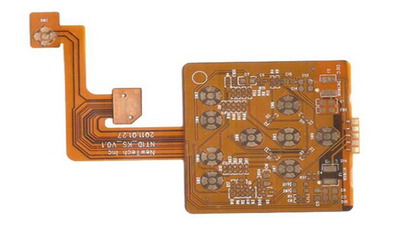
PCB is made by processing a variety of complex process wires and different types of components. The printed circuit board structure is also very complicated, including single layer, double layer and even multiple layers. The production method will be different at different levels. There are many types of circuit boards developed so far. Printed circuit boards can also be classified according to their hardness. There are rigid boards (rigid boards), flexible boards (FPC), and rigid-flex circuit boards. Usually more rigid boards are used. Generally, circuit boards are divided into layers according to the number and thickness of conductive copper foils. They can be divided into single-layer boards, double-layer boards, multilayer boards and double-sided boards. Their structures are also different. Flexible PCB Circuit Board Supplier will introduce their different properties.
Single-layer board structure: This is the simplest structure of the flexible board, usually with a base material + transparent glue + copper foil purchased raw materials, and protective film + transparent glue is another purchased raw material; first, copper The foil needs to be processed by etching and other processes to obtain the required circuit. The protective film is drilled to expose the corresponding pads. After cleaning, the two are combined by rolling, and then the exposed pads are plated with gold or The tin is protected, so that the large board is ready, and then it needs to be stamped into a small circuit board of the corresponding shape.
Double-layer board structure: When the circuit is too complicated, single-layer board cannot be wired, or copper foil is needed for ground shielding, you need to choose double-layer board or multilayer board.
Multilayer Flexible PCB
Multilayer board structure: The most typical difference between a multilayer board and a single-layer board is the addition of a via structure to connect the various layers of copper foil. The first processing process for general substrate + transparent glue + copper foil is to make vias; First, drilling holes in the substrate and copper foil, and then plating with a certain thickness of copper after cleaning, so that the via holes are completed. The subsequent manufacturing process is almost the same as that of the single-layer board.
Double-panel structure: There are pads on both sides of the double-panel, which is mainly used for connection with other circuit boards. Although it has a similar structure to a single-layer board, the manufacturing process is very different. Its raw materials are copper foil, protective film + transparent glue. First, you need to drill holes in the protective film according to the requirements of the pad location, and then paste the copper foil. Then etch out the pads and leads before attaching another drilled protective film.
Although these types of structures of flexible circuit boards are of different types, such as Multilayer Flexible PCB, many manufacturing processes have similarities, but different processes have been added in some basic places to correspond to different fields.
The above is the different structure of PCB circuit board introduced by Rigid PCB Manufacturer. I hope it can help everyone.

没有评论:
发表评论