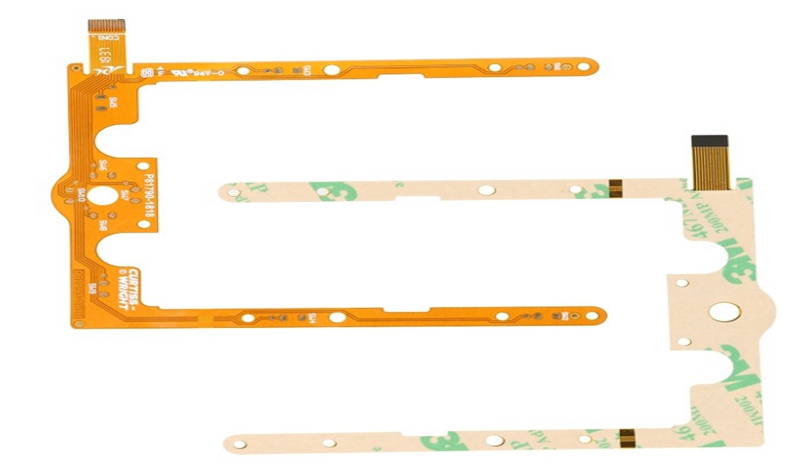
The environmental issues involved in the current PCB production process are particularly prominent. Current topics on lead and bromine are the hottest; lead-free and halogen-free will affect PCB development in many ways. Although at present, the changes in the surface treatment process of PCBs are not very large and seem to be relatively distant, but it should be noted that long-term slow changes will lead to huge changes. With the growing demand for environmental protection, the surface treatment process of PCBs will definitely change dramatically in the future.
The purpose of surface treatment The most basic purpose of surface treatment is to ensure good solderability or electrical properties. Since copper in nature tends to exist in the form of oxides in the air, it is unlikely to remain as copper for a long time, so other treatments of copper are needed. Although most of the copper oxides can be removed with a strong flux in subsequent assembly, the strong flux itself is not easy to remove, so the industry generally does not use strong flux.
Flexible PCB
The five common surface treatment processes now have many PCB surface treatment processes. The five common processes are hot air leveling, organic coating, chemical nickel plating / gold immersion, silver immersion and tin immersion. The following Multilayer Flexible PCB Manufacturer will One by one for everyone.
1. Hot air leveling Hot air leveling, also known as hot air solder leveling, is a process of coating molten tin-lead solder on the PCB surface and leveling (blowing) with heated compressed air to form a layer that is resistant to copper oxidation and can Provides a good solderability coating. heat
2. Organic coating The organic coating process is different from other surface treatment processes in that it acts as a barrier layer between copper and air; the organic coating process is simple and low cost, which makes it widely used in the industry.
3. Electroless nickel plating / gold immersion The chemical nickel plating / gold immersion process is not as simple as organic coating, the chemical nickel plating / gold immersion seems to put a thick armor on the PCB; in addition, the chemical nickel plating / gold immersion process is not like Organic coating serves as a rust-proof barrier layer, which can be useful and achieve good electrical properties during long-term use of the PCB. Therefore, electroless nickel plating / immersion gold is a thick, good electrical nickel-gold alloy wrapped on the copper surface, which can protect the PCB Board for a long time.
4. The silver immersion silver immersion process is between organic coating and chemical nickel plating / immersion gold, the process is relatively simple and fast; it is not as complicated as chemical nickel plating / immersion gold, nor is it a thick layer of PCB Armor, but it still provides good electrical performance.
5. Immersion tin Since all solders are currently tin-based, the tin layer can match any type of solder. From this point of view, the immersion tin process has great development prospects.
6. Other surface treatment processes There are few applications of other surface treatment processes. Let ’s look at the relatively more applied nickel-gold plating and electroless palladium plating processes. Electroplated nickel gold is the originator of PCB surface treatment technology. It has appeared since the emergence of PCB, and it has gradually evolved into other methods. It is coated with a layer of nickel and then a layer of gold on the PCB surface conductor. Nickel plating is mainly to prevent the diffusion between gold and copper.
The above is the surface treatment process of PCB circuit board introduced by Flexible PCB Factory.

没有评论:
发表评论